Hardware
testing involved a systematic approach to built interfacing circuit which is
beginning with testing the component and connection.After the connection is
functional, the full circuit is construct. However, there are a few problems
faced during the hardware development such as the speaker is not functioning
and the connection loss between control panel circuit and GSM modem that cause
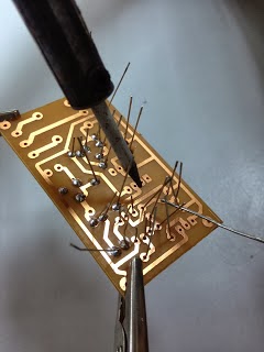
the alert message was not delivered. . Then the circuit was troubleshoot by
changing the speaker and RS 232 cable with the new one and solder it to the
circuit as shown in figure below.
Friday, 25 October 2013
Saturday, 19 October 2013
WEEK 5 (Soldering)
After we had done the PCB processes, we solder the component on the completed UV board. We also tested the components using multimeter.
We do the soldering in our supervisor's lab at level 2, the electronic section.


We do the soldering in our supervisor's lab at level 2, the electronic section.
Friday, 11 October 2013
Friday, 4 October 2013
WEEK 4 (PCB process)
This week, we were doing the cutting & etching process.Plus we also survey the price and components for this project. We have bought all the things needed to process with the next process that is soldering the circuit.


Cutting the UV board

UV board & outline circuit

Etching process
Subscribe to:
Comments (Atom)